Navigating the Precision World of Semiconductor CNC Machining: A Comprehensive Guide
The semiconductor industry, the bedrock of modern technology, demands unparalleled precision and material expertise. While often associated with etching and photolithography, Computer Numerical Control (CNC) machining plays a critical, and increasingly vital, role in the fabrication of semiconductor components and equipment. From creating molds for plastic packaging to manufacturing the intricate housings for testing and handling, CNC machining is indispensable. But machining semiconductors and their related materials isn’t like working with typical metals. This guide will delve into the specifics of semiconductor CNC machining, covering materials, techniques, challenges, and the future outlook.
Why CNC Machining is Crucial in Semiconductor Manufacturing
Traditionally, semiconductors relied heavily on molding and other subtractive processes. However, the increasing complexity of designs, the demand for tighter tolerances, and the need for specialized materials have driven the growth of CNC machining in this sector. Here’s a breakdown of key applications:
- Mold Creation: High-precision molds for plastic encapsulation of integrated circuits require extremely accurate machining.
- Wafer Handling Equipment: Components for wafer chucks, probes, and robotic arms need tight tolerances and compatibility with cleanroom environments.
- Test Fixtures: Custom fixtures for testing semiconductor devices demand rapid prototyping and precise dimensions.
- Heat Sinks & Thermal Management: Efficient heat dissipation is critical for semiconductor performance. CNC machining allows for the creation of complex heat sink geometries.
- Custom Parts & Prototypes: The fast-paced nature of semiconductor R&D necessitates quick turnaround times for custom parts and prototypes which CNC excels at delivering.
- Microfluidic Devices: The increasing use of microfluidics for chemical analysis and biological applications in semiconductor research relies on precision CNC machining.
Materials Commonly Machined in Semiconductor Applications
The materials used in semiconductor manufacturing necessitate specialized machining approaches. Unlike steel or aluminum, these materials often present unique challenges.
| Material | Typical Applications | Machining Considerations | Common Challenges |
|---|---|---|---|
| Aluminum (6061, 7075) | Heat sinks, housings, wafer carriers | Relatively easy to machine, good thermal conductivity. | Burring, chip evacuation. Aluminum is prone to sticking to the cutting tool. |
| Stainless Steel (304, 316) | Fixtures, housings, fluidic components | Good corrosion resistance, requires slow speeds & sharp tools. | Work hardening, necessitating frequent tool changes. |
| Titanium (Ti-6Al-4V) | High-strength components, corrosive environments | Difficult to machine, high heat generation, requires rigid setups. | High tool wear rate, springback. |
| Peek (Polyether Ether Ketone) | Insulators, housings, seals | Exceptional chemical resistance and high-temperature performance. | Tendency to load up the cutting tool, requires specialized geometry. |
| Delrin (Acetal) | Low-friction components, gears, bushings | Excellent dimensional stability and machinability. | Chip evacuation, particularly with long chips. |
| Ceramics (Alumina, Silicon Nitride) | Insulators, structural components | Extremely hard and brittle, requiring diamond tooling and slow speeds. | Cracking, chipping, low tensile strength. |
| Silicon (Single Crystal) | Wafer handling components, test probes | Highly brittle, anisotropic machining characteristics. | Fracturing, surface finish control. Requires specialized grinding and polishing. |
CNC Machining Techniques for Semiconductor Components
The required precision and surface finish in semiconductor applications demand careful selection of machining techniques:
- Micro-Machining: Critical for creating features at the micron or sub-micron level. This often involves specialized micro-tools, high-precision machines, and optimized cutting parameters.
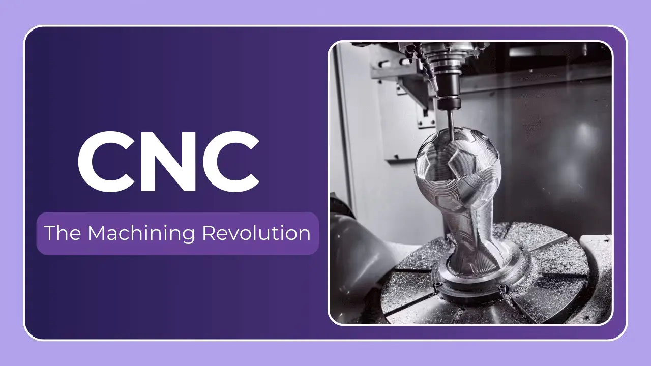
- Five-Axis Machining: Essential for complex geometries and undercuts commonly found in housings and molds. Five-axis machining minimizes setups and improves accuracy.
- High-Speed Machining (HSM): Reduces cycle times and improves surface finish by utilizing high spindle speeds and optimized toolpaths. Requires a rigid machine and stable fixturing.
- Electrical Discharge Machining (EDM): Used for creating intricate shapes in hard or difficult-to-machine materials like tungsten carbide and some ceramics. EDM uses electrical sparks instead of mechanical cutting.
- Swiss-Type Machining: Ideal for producing small, precise, and complex parts in high volumes. A moving guide bushing provides exceptional concentricity.
- Polishing and Lapping: Post-processing steps often required to achieve the extremely smooth surfaces necessary for sealing and optimal performance.
Addressing the Unique Challenges of Semiconductor Machining
Machining materials commonly used in the semiconductor industry presents several unique hurdles:
- Material Brittleness: Silicon, ceramics, and even some advanced plastics can be brittle and prone to cracking during machining. Careful selection of cutting parameters (low cutting speeds, high feed rates) and tool geometry are vital.
- Thermal Expansion: Different materials exhibit varying thermal expansion coefficients. This is critical when machining assemblies of dissimilar materials. Temperature control during machining is essential to maintain dimensional accuracy.
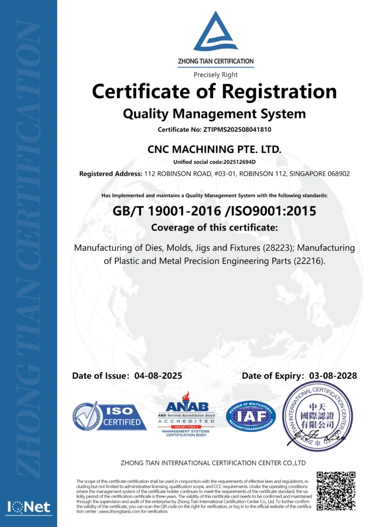
- Cleanroom Compatibility: Many semiconductor components require machining within a cleanroom environment to prevent contamination. This necessitates specialized machines, tooling, and operator protocols. CNC MACHINING PTE. LTD understands these protocols and operations.
- Surface Finish Requirements: Semiconductor applications often demand exceptionally smooth surface finishes to minimize friction, prevent particle generation, and ensure proper sealing. This requires multiple machining passes with progressively finer tooling, followed by polishing or lapping.
- Chip Evacuation: The accumulation of chips can lead to dimensional inaccuracies and tool damage. Effective chip evacuation systems are crucial, particularly when machining aluminum and plastics. Air blasts and coolant selection play a key role.
- Tool Wear: Hard and abrasive materials (like ceramics) rapidly wear cutting tools. Regular tool inspection and replacement are essential to maintain accuracy and surface finish.
Importance of Precision, Fixturing, and Quality Control
The semiconductor sector isn’t forgiving of errors. Precision is paramount.
- High-precision Machines: 5-axis CNC machines with sub-micron accuracy are standard.
- Rigid Fixturing: Minimizing vibration is crucial. Robust workholding solutions are employed to ensure stability.
- Advanced Tooling: Diamond-coated tools, micro-drills, and specialized end mills are commonly used.
- In-Process Inspection: Using CMMs (Coordinate Measuring Machines) and optical comparators to verify dimensions during the machining process.
- Statistical Process Control (SPC): Monitoring key process parameters to ensure consistent quality and identify potential issues early.
- Material Certification: Ensuring the materials used meet the stringent purity and composition requirements of semiconductor applications.
The Future of CNC Machining in Semiconductor Manufacturing
CNC machining’s role in the semiconductor industry is poised to expand. Several emerging trends are driving this growth:
- Advanced Packaging: As semiconductor devices become more complex, advanced packaging techniques (like 2.5D and 3D integration) require increasingly sophisticated machining capabilities.
- Heterogeneous Integration: The integration of different materials and technologies into a single device demands versatile machining solutions.
- Micro-LED Manufacturing: CNC machining is playing a crucial role in the fabrication of micro-LED displays, requiring high-precision micro-milling and structuring.
- Industry 4.0 Integration: The integration of CNC machines with digital twins, AI-powered process optimization, and predictive maintenance will further enhance efficiency and quality.
- Additive Manufacturing Hybridization: Combining CNC machining with additive manufacturing (like 3D printing) allows for the creation of complex geometries with near-net-shape precision. The CNC machine can then be used to finish the additively manufactured part to the necessary tolerances and surface finish.
Conclusion
CNC machining is no longer just a supporting process in semiconductor fabrication; it’s a fundamental enabler of innovation and progress. Successfully navigating this specialized field requires a deep understanding of materials, precise machining techniques, rigorous quality control, and a commitment to continuous improvement. Choosing a partner with the right expertise and capabilities, like CNC MACHINING PTE. LTD in Singapore, is critical. We offer advanced five-axis CNC machining, comprehensive post-processing services, and a dedication to delivering customized precision parts quickly and efficiently, at the best price – making us the first choice for your semiconductor manufacturing needs. Don’t hesitate to contact us to discuss your project and experience the difference precision engineering can make.


